
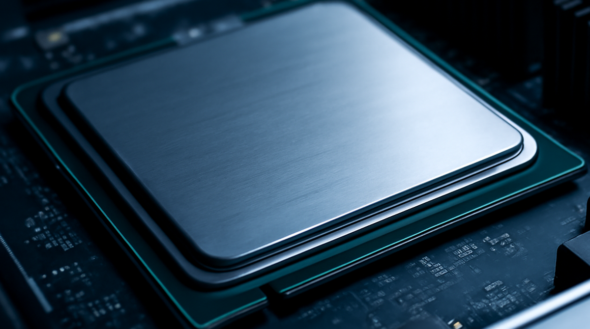
On May 21, 2026, AMD announced that it had begun production ramp of its next-generation server processor codenamed "Venice"[1]. Venice, the company's 6th Gen EPYC processor, is manufactured on the most advanced 2nm process from TSMC (Taiwan Semiconductor Manufacturing Company), and is the first high-performance computing (HPC) product in the industry to reach production on the 2nm node[1]. With demand for AI infrastructure climbing as agentic AI spreads, AMD frames the milestone as a step forward in executing its data center CPU roadmap[1].
Industry-First HPC Product in Production on TSMC 2nm
According to AMD, production of Venice is underway at TSMC's facilities in Taiwan, with plans to also ramp production at TSMC's fabrication site in Arizona[1]. AMD says that building manufacturing capacity in both Taiwan and Arizona is intended to strengthen a geographically diverse footprint for advanced manufacturing[1].
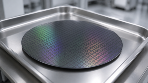
The 2nm process used to build the chip is the leading-edge manufacturing technology that TSMC moved into volume production in the fourth quarter of 2025[2]. Adoption is expanding beyond smartphones to large-scale designs for AI and the data center, and AMD is bringing an HPC product to the node in its early phase[1][2]. TSMC has also signaled that it will move up the timing of 2nm production in Arizona to 2027[2].
As a 6th Gen EPYC processor, Venice is designed to raise the processing performance and power efficiency required for cloud, enterprise systems, HPC and AI workloads[1].
Agentic AI Raises the Role of the CPU
AMD describes this production ramp as an important step amid the accelerating buildout of AI infrastructure[1]. Dr. Lisa Su, chair and CEO, said that ramping "Venice" on TSMC's 2nm process is an important step forward in accelerating the next generation of AI infrastructure, and explained that the partnership with TSMC supports the speed and scale of bringing products to market[1].
AMD notes that as AI use expands from training and inference toward more complex agentic workloads, the role of the CPU becomes even more important[1]. The view is that the CPU, which coordinates data movement, networking, storage, security and overall system orchestration within the data center, is becoming indispensable for scaling AI infrastructure[1].
Dr. C.C. Wei, Chairman and CEO of TSMC, which handles the manufacturing, also commented that he is pleased to see AMD making strong progress with its next-generation EPYC processor using TSMC's advanced 2nm process technology, adding that pairing leading process technology with design supports high-performance and AI computing[1].
The Follow-On "Verano" and the Data Center Roadmap
AMD also indicated that it will extend TSMC's 2nm process across its entire data center CPU roadmap[1]. "Verano," the follow-on to Venice, is positioned as a 6th Gen EPYC processor as well, aimed at leadership in performance per dollar and power efficiency[1]. AMD says Verano plans to incorporate advanced memory technologies, including LPDDR memory, for workloads where power constraints are tightening[1].
The collaboration between AMD and TSMC extends beyond the 2nm process to advanced packaging technologies such as SoIC-X and CoWoS-L, used across a broad range of AMD's AI and data center product lineup[1].
According to the data center roadmap AMD has disclosed to date, Venice adopts the new "Zen 6" architecture and supports up to 256 cores[3]. This announcement shows that those plans have entered the concrete stage of production[3].
Summary
AMD has begun production of its next-generation EPYC "Venice" on TSMC's leading-edge 2nm process. It is the industry's first HPC product in production on 2nm, with manufacturing planned in Arizona following Taiwan. As the importance of the CPU grows with the spread of agentic AI, attention turns to how the roadmap, including the follow-on "Verano," will unfold.