
Intel CEO Lip-Bu Tan has once again voiced interest in the memory business, this time on a podcast. Coming from a company that walked away from DRAM in 1985, that is a loaded remark. And around Intel, three separate moves have been advancing in parallel during the first half of 2026 alone: a patent for a new architecture called XBM, joint development of ZAM with a SoftBank subsidiary, and the hiring of a former SK hynix CEO.
※1 USD = 158 JPY
Returning to a Market It Chose to Leave
When Intel was founded in 1968, memory chips were its only products. It shipped the industry first commercial SRAM, the 3101, in 1969, and its first commercial DRAM, the 1103, the year after. Intel is a CPU company today, but it started life as a memory maker.
The turn came in the early 1980s. Japanese manufacturers arrived with overwhelming volume manufacturing, and DRAM prices kept falling. With the economics no longer working, Intel exited in 1985. For decades that decision was held up as the right call: flee the commodity, concentrate resources on microprocessors. It became a famous case study in management education.
AI Turned Memory Into a Strategic Resource
AI has undone that premise. Bandwidth demand from AI accelerators has exploded, and High Bandwidth Memory (HBM) is now the bottleneck in every AI chip. HBM accounts for only about 8 percent of DRAM bit shipments, yet it generates roughly 30 percent of DRAM revenue. Supply sits almost entirely with three companies: SK hynix, Samsung and Micron.
The price outlook is no gentler. Gartner projects that DRAM and SSD prices will climb 130 percent by the end of 2026. Tan himself said back in February 2026 that major memory suppliers had told him there would be no relief until 2028. Memory is no longer a part you simply buy cheaply and mount on a board.
XBM: Throwing Out the Silicon Interposer Entirely
A patent Intel filed on December 26, 2024, and published on July 2, 2026, describes a structure called cross-batch memory (XBM).
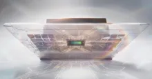
Conventional HBM stacks DRAM dies on a silicon interposer and talks to the processor over an extremely wide 1,024-bit parallel interface. XBM does away with the interposer. The DRAM cells themselves are built as thin-film transistors in the back-end-of-line (BEOL) metal layers above the transistor layer, and data moves over a UCIe serial link at 32 GT/s. Each die holds roughly 1.5 GB, so an 8-layer stack reaches 12 GB, with the design extending to 16 layers. Built-in self-repair (BISR) and spare channels are baked in from the start to address stacking yield.
The point of the approach is that it removes the interposer and micro-bump bonding, the very elements that have kept HBM expensive, at the design stage. Commercialization, however, is not expected until 2030 or later, and this remains a patent.
ZAM: Nine Bonded Layers With SoftBank Subsidiary SAIMEMORY
The second thread is ZAM (Z-Angle Memory). On February 2, 2026, Intel signed a collaboration agreement with SAIMEMORY, a SoftBank subsidiary.
ZAM uses fusion bonding to stack nine layers of DRAM, thinning the silicon between layers to about 3 micrometers to cut TSV resistance. Data presented at the 2026 VLSI Symposium put bandwidth density at roughly 0.25 Tb/s/mm2, which works out to about 5.3 TB/s for a 10 GB module. HBM4 delivers roughly 2 TB/s per stack, so this is more than double. Energy per bit moved is said to be under 0.7 picojoules.
Japan Ministry of Economy, Trade and Industry is providing subsidies of up to 3.8 billion yen, with prototypes targeted for fiscal 2027 and commercialization for fiscal 2029. That timeline is more concrete than XBM, but it is still several years out.
The People and the Money Are Already Moving
The personnel move is the interesting part. On June 18, 2026, Intel appointed Seok-Hee Lee as executive vice president of Intel Foundry. Lee worked on process integration at Intel from 2000 to 2010, then led HBM development as CEO of SK hynix. He was also on the buying side when SK hynix acquired Intel NAND business for 9 billion USD (about 1.4 trillion yen) in 2020. The executive who bought the business is now back at the company that sold it.
On the funding side, Intel upsized a stock offering originally planned at 15 billion USD to 20 billion USD (about 3.2 trillion yen) on August 10, 2026, pricing shares at 95 USD. Net proceeds came to roughly 19.7 billion USD. The stated use is general corporate purposes including capital expenditures and working capital, with no mention of memory. Still, Tan memory comments surfaced on August 12, the day that offering closed.
Three Retreats Already, and a Fourth to Avoid
1985 was not Intel only painful memory episode. It bet on Rambus RDRAM in the late 1990s and pulled out in 2001. It brought 3D XPoint to market as Optane in 2017 with Micron and discontinued it in 2022. Optane alone accumulated losses of about 6.8 billion USD (about 1.07 trillion yen) between 2016 and 2020. The NAND business is already sold.
What separates this attempt from the previous three is that it is not about mass-producing conventional DRAM or NAND and slugging it out on price. XBM and ZAM are both proposals to rebuild the cost structure underneath HBM, which looks less like stepping into the existing arena than reshaping the arena itself.
Even so, a patent is not a product. Between a ZAM prototype in fiscal 2027 and XBM commercialization in 2030 or later, HBM4E and HBM5 will arrive, and SK hynix and Samsung will not sit still. Because the AI accelerator ecosystem is optimized around HBM, moving to a different architecture would require the whole industry to move together. Tan himself declined to clarify whether this is an official Intel strategy or a personal interest, saying only that they are not ready to unfold it.
Summary
The company that invented DRAM is reconsidering that field 40 years after leaving it. XBM rebuilds the interconnect, ZAM rebuilds the bonding method, each from the ground up. The fact that a patent, a joint development deal, an executive hire and a capital raise all landed in the same six months suggests this is more than a passing thought. At the same time, the schedule points to a prototype in fiscal 2027 and commercialization from fiscal 2029 to 2030 and beyond. Whether this becomes a third attempt or a fourth retreat should become clear from the concrete investment decisions of the next two years.