
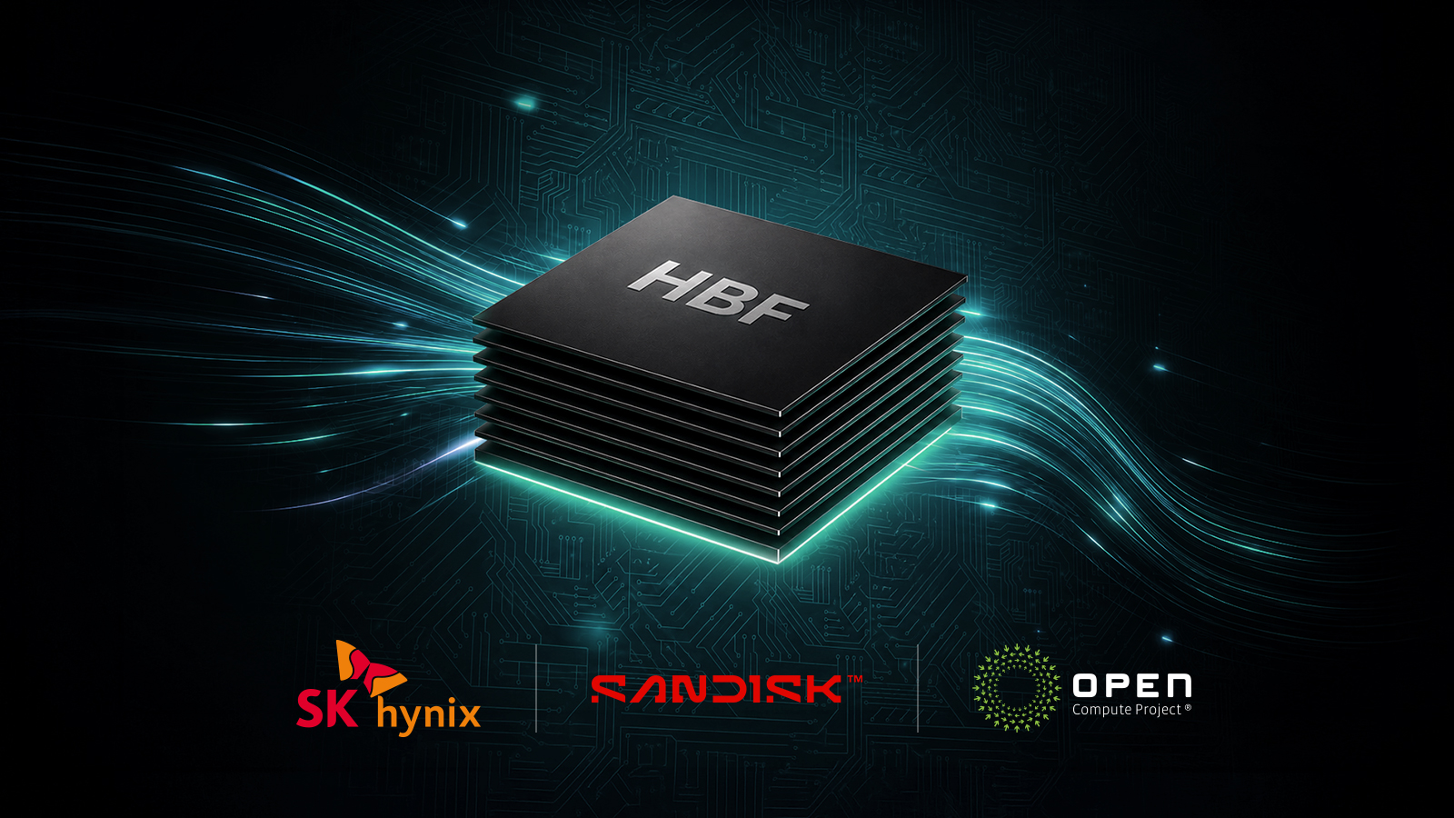
SK hynix and Sandisk have published the first standard specification for High Bandwidth Flash (HBF), a next-generation storage technology. The idea is to stack NAND flash right next to an AI accelerator so it can deliver HBM-class transfer speeds with far more capacity. The spec defines up to 512GB per stack and up to roughly 3TB/s of bandwidth, and it was released through the Open Compute Project (OCP) so anyone can build against it.
Adding One More Layer Between HBM and SSDs
Today's AI servers usually place HBM (High Bandwidth Memory) directly beside the GPU, with SSDs sitting further out. HBM is fast but capacity-limited, while SSDs offer capacity at the cost of speed. That leaves only two layers with very different characteristics.
The gap between them becomes a problem as inference scales up. Model weights and context data no longer fit in HBM, and reaching all the way out to an SSD means waiting. HBF is designed to sit in that middle ground. Stacking NAND vertically provides the capacity, while the interface targets bandwidth closer to HBM levels.
It is worth being clear that SK hynix and Sandisk are not positioning HBF as a replacement for HBM. The specification assumes the two coexist in the same system, with HBM handling latency-sensitive work and HBF holding the bulk data, such as model weights, that needs to stay close at hand.
Up to 512GB, With Three Bandwidth Grades
The published spec defines two stack configurations, using either 8 or 16 stacked NAND dies, covering capacities up to 512GB. Bandwidth is split into three tiers, Grade 1 through Grade 3, scaling from roughly 0.4TB/s to 3.0TB/s.
The tiered approach reflects the fact that HBF is not meant for a single product but for a range of accelerators. Beyond capacity and bandwidth, the specification covers connection interfaces and electrical characteristics, reliability and packaging guidance for the HBF die stack process, and software I/O guidelines. In short, it supplies the pieces an implementer needs.
Sandisk has previously indicated that a 16-die stack can reach 512GB in a package roughly the same size as HBM. The company has also claimed HBF could offer 8 to 16 times the capacity of HBM at comparable cost, and said its own simulation using Llama 3.1 405B landed within 2.2 percent of a system with unlimited HBM capacity. Those are vendor figures, but they show what the technology is aiming for.
UCIe for the Interconnect, Usable With GPUs and CPUs
One notable choice in the specification is UCIe (Universal Chiplet Interconnect Express) as the link to the processor. UCIe is an industry standard interface designed for high-speed connections between heterogeneous semiconductor chiplets, not a proprietary format tied to one vendor.
Standardizing here means HBF can be paired with CPUs and other processor types, not just GPUs. Combined with the decision to publish through OCP, the intent is clearly to establish shared industry infrastructure rather than a walled garden.
Six Months to a Spec, With Google and Tenstorrent on Board
SK hynix and Sandisk first partnered on standardization in August 2025, and the consortium launched in February 2026. Reaching a first specification roughly six months later is quick by semiconductor standards.
Google and Tenstorrent have since joined the consortium. Having companies that actually design and operate AI accelerators involved, rather than memory vendors alone, matters for how workable the spec turns out to be. The earlier those requirements land, the less likely the standard is to stay theoretical.
On timing, Sandisk has previously pointed to first samples in the second half of 2026, with AI inference devices using HBF sampling in early 2027. The latest announcement does not update that schedule. For now, the point is that a shared interface exists ahead of commercial parts, so developers can design against the same assumptions.
A 375-Layer NAND Debut at FMS 2026
The announcement coincides with FMS (Future of Memory and Storage) 2026, running August 4 to 6 at the Santa Clara Convention Center in California. On the opening day, SK hynix's Kim Chun-sung and Kang Uk-song deliver a joint keynote on Tiered Memory, the idea of connecting multiple memory types into a single optimized system. A panel discussion with Sandisk and Google DeepMind follows on August 6.
At its booth, SK hynix will show its tenth-generation 375-layer 4D NAND wafer and products for the first time. The company says performance per watt improves 2.5 times over the previous generation, and it plans to move high-performance, high-capacity eSSDs based on that NAND into mass production in the first half of 2027. The new memory layer and the NAND generation underneath it are being shown at the same event.
Summary
The first HBF specification from SK hynix and Sandisk defines up to 512GB of capacity, up to roughly 3.0TB/s of bandwidth, and UCIe as the processor interconnect. Rather than replacing HBM, it adds a layer between HBM and SSDs to ease the capacity squeeze during inference. Google and Tenstorrent have joined the consortium, and the spec is open via OCP. Actual products are still ahead, but this marks the point where AI memory started moving from two tiers to three.