
NTT has published results from an experimental platform that lets AI and robotics search for thin-film growth conditions without human intervention. Working on beta-phase gallium oxide, a promising next-generation power semiconductor material, the system runs deposition, evaluation, and the choice of the next condition in a closed loop, roughly tripling the pace of the experimental cycle. The striking part is what happens after the optimum is found: the platform also extracts growth rules that a human can read and carry over to other work.
The AI picks the condition, the equipment simply follows
How a thin film is grown largely determines what a semiconductor material can do. A small shift in temperature, applied power, or gas flow changes film quality, and those conditions interact with one another in complicated ways. For a long time this was territory where experienced researchers closed in on the answer through intuition and accumulated practice.
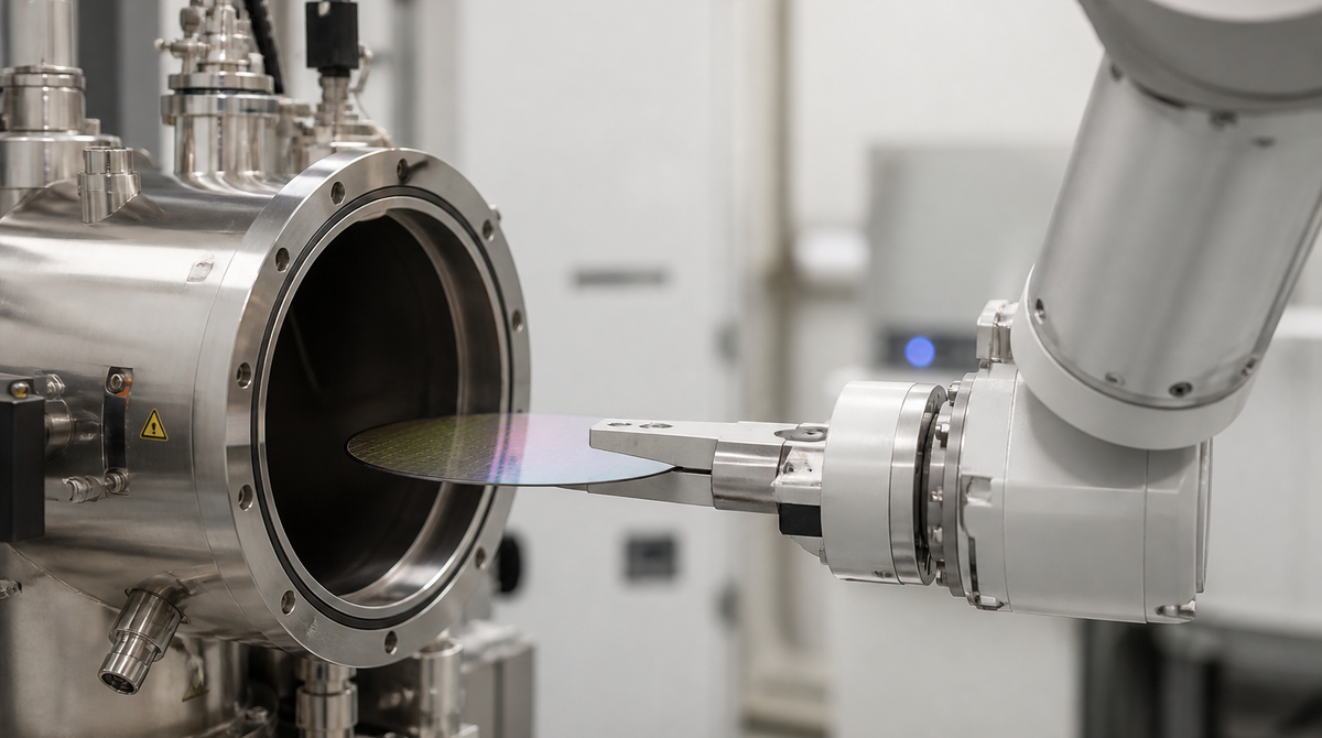
The new platform hands that closing-in work to the equipment. Wafers are transported automatically inside the sputtering chamber, films are grown under conditions proposed by Bayesian optimization, and the resulting film is measured optically and scored automatically. That score feeds back into the prediction model, which selects the next condition. The loop keeps turning without waiting for human analysis. Four deposition parameters were varied: temperature, sputtering power, argon flow, and oxygen flow.
Compared with the era when a researcher performed each run by hand, one lap from deposition to evaluation now takes roughly one third of the time. The equipment did not get faster. What disappeared was the human waiting time between thinking about a condition and setting up the next run.
Beta-phase gallium oxide had been a hard case for sputtering
The demonstration target, beta-phase gallium oxide (β-Ga₂O₃), has a bandgap of about 5 eV. That wide gap makes it tolerant of high voltages and responsive to short-wavelength ultraviolet light, which is why it keeps coming up as a candidate for next-generation power devices.
The difficulty is in making it. Sputtering suits large-area, low-cost production and sits well with volume manufacturing, but high-quality single-crystal films of this material had been out of reach with that method. The team therefore worked in two stages, first searching for conditions on a sapphire wafer and then transferring the conditions found there to deposition on a β-Ga₂O₃ substrate.
Film quality was judged by Urbach energy, which reflects defects and disorder in atomic arrangement, and the search aimed at lowering that value. After 56 autonomous iterations the platform reached 182 meV, described as the lowest value reported for a sputtered β-Ga₂O₃ film. Heteroepitaxial growth consisting only of the intended crystal phase was confirmed as well, making this the first single-crystal β-Ga₂O₃ thin film obtained by sputtering.
Getting out of the black box
Up to this point, AI-driven condition search is not unusual. The dividing line comes next.
The condition and quality data accumulated by the autonomous loop were analyzed with a random forest, an ensemble method that combines many decision trees. Its predictions were then decomposed into the contribution of each parameter and the interactions between parameters. What looked like complicated variation in film quality turned out to be mostly explainable by adding up the individual effects of temperature, power, argon flow, and oxygen flow. The only pairing that simple addition failed to capture was temperature and oxygen flow.
The resulting guideline was to adjust each parameter in turn and then concentrate on temperature and oxygen flow at the end. When researchers re-optimized along that rule, Urbach energy fell further to 163 meV. The extracted rule was therefore not an after-the-fact explanation but a workable guide, and the result demonstrated it.
If the answer an AI produces can be translated into a form humans can accept, it can be carried across to other materials and other equipment. NTT frames the work as a step beyond automating condition search and into producing scientific knowledge.
What still needs hands, and what comes next
This is not full unattended operation. In the current configuration, people are still involved in setting wafers into the load lock and in part of the transfer of deposited samples to the optical measurement stage. How far to automate handoffs between instruments is a shared assignment for self-driving labs of this kind.
NTT says it will move on to optimization that handles multiple evaluation metrics and to AI models that incorporate knowledge of material properties and deposition processes. A phase of broader validation across more materials and more equipment lies ahead, and whether the same procedure holds up on other institutions' hardware remains to be seen. The work was published in Nature Communications on August 13, 2026.
Summary
The value of autonomous experimentation has so far been framed as reaching the optimum quickly. NTT's demonstration adds a second claim: that researchers can take home an understanding of why a given condition works. Reaching a single-crystal film by sputtering on a material as awkward as β-Ga₂O₃, and then improving the number further using the extracted rule, are the two facts that support it. The result is a reminder to ask where the real bottleneck in materials development actually sits.