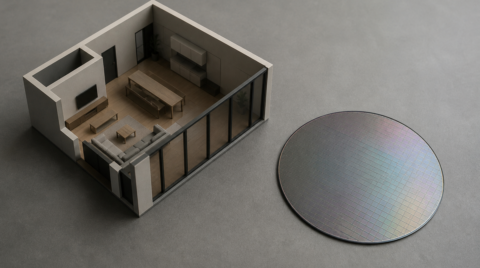

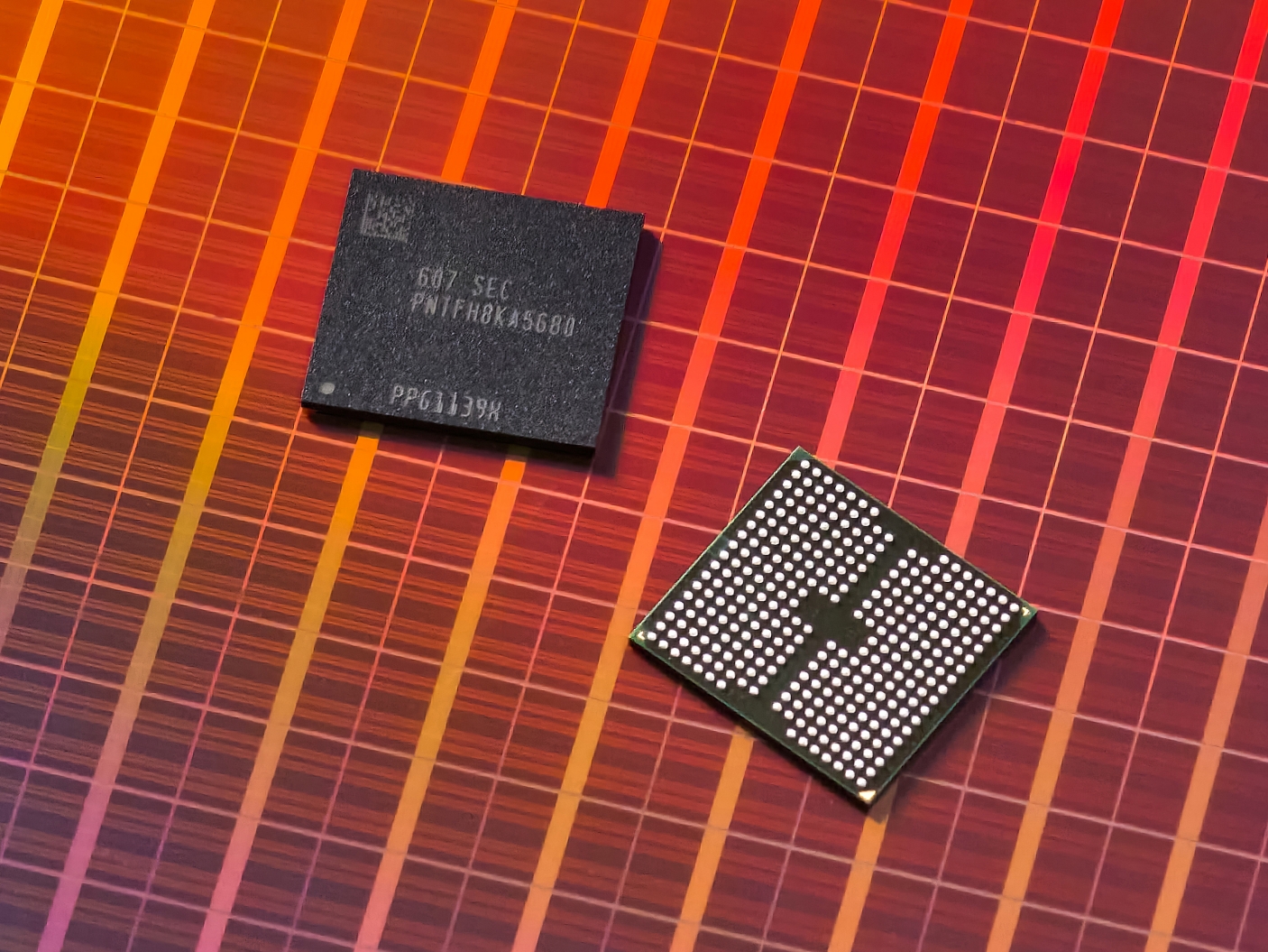
SAMSUNG laid out its next-generation 3D memory plans at Future of Memory and Storage (FMS) 2026 in Santa Clara, California. The centerpieces are two concept models: zHBM, which stacks HBM directly on top of an AI accelerator, and zNAND-O, a fast NAND aimed at edge AI. The company also showed V10 BV-NAND, with more than 400 layers, for the first time in the industry.
Stacking HBM Directly Above the AI Accelerator
Today's HBM sits alongside the AI processor. zHBM breaks that assumption by stacking HBM vertically, directly above the accelerator. Shortening the physical distance data travels between processor and memory is meant to lift both bandwidth and power efficiency.
The figures SAMSUNG put forward are ambitious. A next-generation interface built around zHBM is expected to deliver roughly 8 times the performance of HBM5. Paired with next-generation wafer bonding, the company says memory density can exceed 10 times that of HBM5, energy efficiency can improve threefold, and thermal resistance can drop by more than half. In high-capacity, high-bandwidth configurations, heat directly determines operating stability, which makes the thermal figure as meaningful as the bandwidth one.
The interesting part is that zHBM assumes per-customer variation. Custom IP can be integrated into the interposing layer between the memory and the AI accelerator. Memory is shifting from a general-purpose component toward a part tailored to a specific accelerator design.
zNAND-O for Edge AI
The second concept model is zNAND-O, a high-performance NAND built on the company's V-NAND technology. Four-layer and eight-layer versions are currently in development.
Its target is not the data center but edge AI, where real-time processing happens on the device. The design chases space efficiency, I/O performance and low latency at the same time, for workloads that ingest data and run inference on the spot. If zHBM supports AI training and large-scale inference, zNAND-O is the part that keeps AI running in the field.
V10 BV-NAND Raises Density by 58 Percent
Unlike the concept models, V10 BV-NAND appeared as a product. It uses a new Bonding V-NAND architecture and exceeds 400 layers, the first time this structure has been shown publicly by anyone in the industry.
Wafer bonding is the key. Applying it to the process of stacking memory cells raised memory density by roughly 58 percent compared with the previous V9 generation. Read, write and I/O performance also improve over the prior generation.
SAMSUNG introduced its first V-NAND at the 2013 Flash Memory Summit. Thirteen years later, the stacking method itself is being replaced by bonding.
A Roadmap from HBM4E to LPDDR5X-PIM
Beyond the concept models, the booth featured HBM4E, HBM5, LPDDR5X-PIM and enterprise storage such as the PM1763 and BM1773. Roughly 30 technologies were on display in a booth styled after an AI cloud server.
On HBM, the company says it was first in the industry to begin mass production of HBM4 using 1c DRAM and a 4-nanometer base die in February 2026, and first to ship HBM4E samples in May. LPDDR5X-PIM brings processing-in-memory to the LPDDR family, another industry first. The idea is to cut the number of times data has to move at all, saving both transfer time and power.
The keynote was delivered by Jin-Yub Lee, who heads Flash Product and Technology, and Kyungryun Kim, project leader of the DRAM design team. As an integrated device manufacturer with memory, foundry and advanced packaging in house, SAMSUNG is pitching a one-stop path from design to mass production.
Summary
At FMS 2026, SAMSUNG presented three pillars: zHBM stacked above the AI accelerator, zNAND-O for edge AI, and the 400-plus-layer V10 BV-NAND. All three move away from arranging memory across a plane and toward the question of how to stack and bond it vertically. Whether the claimed 8 times HBM5 figure holds up in shipping hardware remains to be seen, but the race to raise AI infrastructure performance from the memory side looks set to continue.