
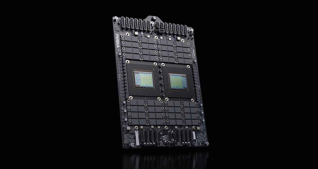
NVIDIA has revealed that it is putting its own server-class "Vera" CPU to work in the electronic design automation (EDA) workflows used to design its next-generation CPUs and GPUs. Working with EDA leaders Cadence and Synopsys to optimize their applications, the company says it has seen up to 1.5x speedups on parts of the verification process[1]. The aim is to create a loop in which NVIDIA's own chips help build its next chips.
Even in a GPU-first design flow, some stages still lean on the CPU
Modern chip design grows more complex the more advanced the CPUs, GPUs and AI systems that teams try to build. Long before manufacturing, engineers spend years validating behavior, identifying corner cases and refining designs across thousands of iterations[1].
Simulation, verification and implementation sit at the center of semiconductor development. While GPUs and AI have accelerated many parts of the flow, logic simulation, formal verification and portions of digital implementation still depend heavily on CPU performance — fast individual cores, efficient memory and strong overall throughput[1].
That makes CPU architecture a key factor in how quickly a team can validate designs, explore alternatives and move toward tapeout (handing the design data over to manufacturing). Even in an AI-era design flow dominated by GPU headlines, some stages still test the raw strength of the CPU.
Up to 1.5x with Cadence and Synopsys tools
NVIDIA's initial testing focused on leading EDA applications[1].
One is Cadence Jasper, a formal verification platform that uses smart proof technology and machine learning to find and fix bugs early in the design cycle and improve verification productivity[1]. The other is Synopsys VCS, a high-performance functional verification solution that simulates and validates complex chip designs before fabrication. Both ran on the same number of cores in the test[1].
Both applications showed up to 1.5x higher performance on selected workloads[1]. Beyond the benchmark numbers, NVIDIA says it is working closely with both companies on application profiling, software optimization and system-level tuning to lift productivity across a broader range of workflows[1]. That said, these are figures from NVIDIA's own testing; the detailed comparison conditions and settings have not been disclosed, so there is no guarantee the same results carry over to other environments.
Rolling Vera out across the design flow
The Vera CPU being deployed combines 88 custom Olympus cores with a high-efficiency LPDDR5X memory subsystem and a second-generation NVIDIA Scalable Coherent Fabric[1]. It is built to deliver strong per-core performance, high memory bandwidth and consistent low latency for demanding design applications. Vera was originally introduced in March 2026 as a CPU for AI factories, and NVIDIA has now extended its role onto its own design floor[1].
These traits matter most for workloads that mix latency-sensitive jobs with large-scale regression testing spread across compute farms[1]. Faster execution shortens individual verification runs, while greater throughput lets engineers evaluate more design alternatives and complete more validation within the same development window. In a field where the number of design iterations directly shapes a product's maturity, those gains add up.
A loop where NVIDIA chips build the next NVIDIA chips
After defining a processor's architecture and microarchitecture, engineers describe much of its behavior at the register-transfer level (RTL). From there, logic simulation, formal verification, regression testing and digital implementation work together to turn the design into manufacturable silicon[1].
Because these stages are interconnected, higher verification throughput helps surface issues earlier and reduces costly downstream rework[1]. Behind deploying Vera across its entire design flow is a philosophy of assigning each task to the compute best suited to it. In EDA, GPUs and AI accelerate many algorithms, while high-performance CPUs handle the critical simulation, verification and implementation — the two working together to speed the overall design cycle[1].
By using its own CPUs to design its next-generation CPUs and GPUs, NVIDIA says it is building a continuous feedback loop among silicon design, software optimization and systems engineering[1]. Looking ahead, it plans to build on Vera with the next-generation Rosa CPU, powered by the Rigel core[1]. Related work will also be shown at DAC 2026, the international design automation conference held July 26–29 in Long Beach, California[2].
Summary
NVIDIA has put its Vera CPU into the EDA workflows used to design next-generation CPUs and GPUs, showing up to 1.5x speedups with Cadence's and Synopsys's verification tools. With 88 Olympus cores, Vera handles the formal verification and simulation where CPU performance counts, sharing the load with GPUs and AI. The goal is a loop where NVIDIA's chips build its next chips, with the Rigel-based Rosa CPU up next. The performance figures come from the vendor, so third-party verification is still warranted.